Radio

It’s been forever since I did an update. A lot of my stuff is in video form on youtube now. If anyone is still reading this blog, please leave a comment (even if you don’t have much to say).

Anyway, something that I’ve been looking for, for the longest time is a high speed ethernet data modem that works on either VHF or UHF low band (50 – 500 MHz). Such a device would be essential to have in either developing countries or areas where internet is hardly accessible. The VHF low band is empty now. Keep in mind that this is probably not legal in the land of the “free”, so this should only be implemented in other countries. However, testing with only a few mW in the 72 – 76 MHz license free band – I believe 1W is allowed here, but please check.

(Side Note: Part of the reason why everything is made in China is NOT just the low cost, but it’s the lack of ancillary rules that prevent efficient cheap production and innovation. Something like this would be very useful, but nope, the psychos say we can’t do it. Ham radio was meant to be about experimentation, but now there is very little actual innovation because all the rules are set. Now it’s just a place for people who want to use pre-made stuff or if they do build their own, it has to be a specific way that doesn’t allow for new developments. Now SDRs have opened a gateway to endless possibilities, but most of which would not be allowed.)

~70 MHz is a perfect frequency to use because it travels long distances with little power. It’s not so low that it begins to act like HF however and bounces off the ionosphere causing distortion. I believe it to be the best band for a high speed data link. The system could use QAM64 or other QAM to send data fast with lower bandwidth usage. 1 MB/s should be easily attainable and it will use way less bandwidth than a TV station.

When you go searching for radio data links, you’ll either find some really cheap Chinese RS232 or 485 serial port modems that claim speeds of up to 115kbps (which is the max for serial) or you’ll find expensive boxes made by companies that are too afraid to show you the price 🙂 The speeds of the Chinese are a complete lie. These devices can only transmit data at around 1 KB/s max. I’ve tested several of them. This may be good enough for a simple texting program however. I actually made one a few years ago that even had PGP integrated, but it was buggy and too slow to send anything other than text messages.

So I believe the best way forward is to use the LimeSDR. Many SDRs don’t even transmit, but most of the ones that do are not very clean (unless you’re talking about the elite ones, like ettus research). The Lime should be clean and it works with GNU radio which is what I’ll be using to implement the data link. The great thing about GNU radio is that it is a visual block diagram type programming system for digital radio. You can make literally anything you want in there. Including an old fashioned ham SSB transceiver, etc. The only thing I don’t like is that it seems buggy on Windows. GNU radio also appears to have an ethernet source/sink. This means it can interface with an ethernet port using what I think is called Tun-Tap. This should make it possible to send data from the ethernet port directly into the radio. Will it work? I have no idea because the information on using this part of the software is very sparse. I know the QAM part of it will work though. It’s just a matter of getting the Ethernet data in. There’s a guy who demonstrates using the LimeSDR to send files here: http://coolsdrstuff.blogspot.com/2018/08/transmitting-with-limesdr-mini.html

If the ethernet part doesn’t work, I can always use it just to interface with my chat program. It’s kind of like telegram (the software). Where you can text and send data/image attachments. This part may be more practical if the ethernet link doesn’t work.
I just wanted to let you know that I’ve added some RF calculators to the side panel of this website.

I use them almost daily when doing radio projects. Some of them are adapted from other websites and some are my own. They are all programmed in javascript, so no need to download anything.

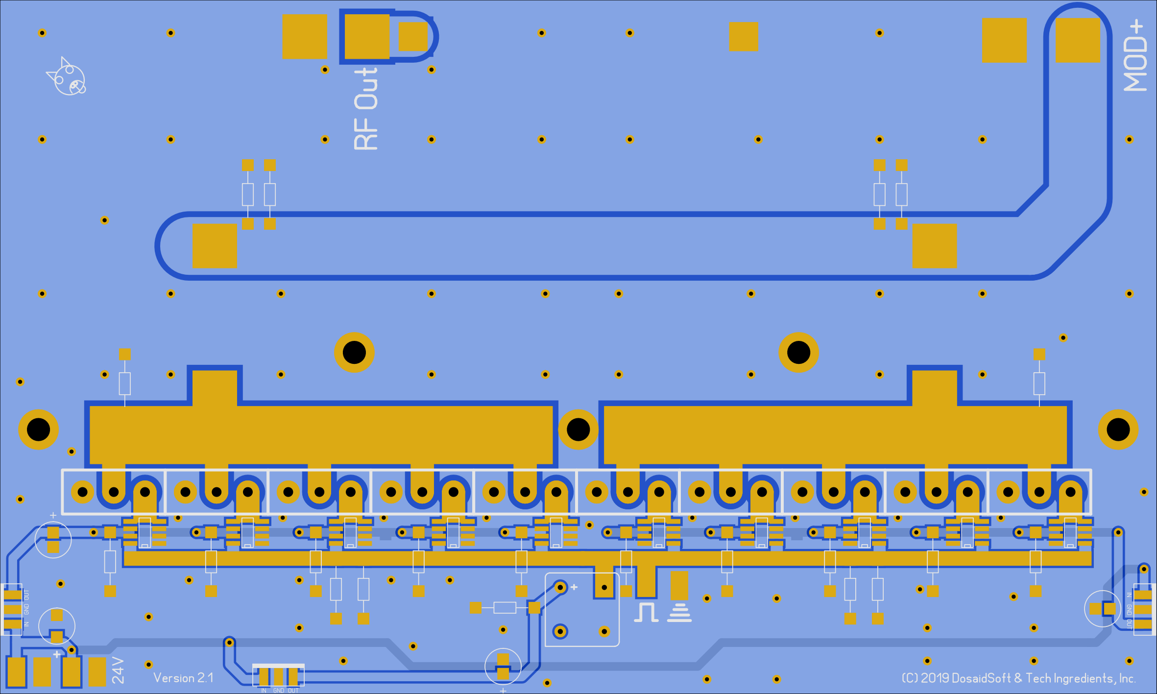
I am back after a little hiatus to give a quick update on the transmitter. The new V2 transmitter board has proven to be flawed after some testing. It has been tested and shown that the long clock traces are rounding the waveforms a bit too much. I am going to update this post with the new V2.1 which will correct the issue.

In addition to the clock trace problem, the new NCP 8-SOIC surface mount drivers are a bit more demanding in their heat dissipation requirements than I thought. The new V2.1 board will require some small heastinks on the drivers to prevent overheating. The drive voltage has also been decreased to 15V instead of 18V because it has been proven to be just as efficient operating at 15V and the drivers get a little less hot.

So the changes in V2.1 will be:

  • Shorter clock traces
  • Heatsinks required on drivers
  • Voltage changed to 13.7V or 15V on the drivers
  • Inverter chip removed (integrated inverted inputs on drivers used instead)

Stay tuned for an update. And please post a comment if you have anything to offer, I’d like to get an idea if anyone is still reading this blog. I will continue to update it regardless, however.

Update:

I am sending the V2.1 to fabrication and they should be done in a few weeks; I will then begin the testing. I believe they will work much better. I still think there may be an efficiency problem with the output match. I might need to change to using coax in the balun instead of wire. I am not sure how this is done though, so I will do some research.

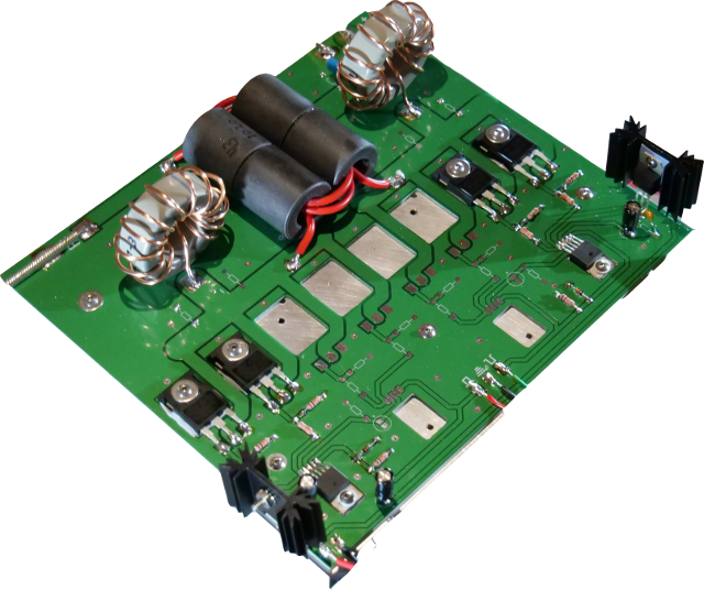
Here is a photo of the V2.1 board:

The latest version of the transmitter board has just finished production and will be arriving soon.

The new version has several improvements over the last. It is now using the NCP drivers and using one of those per MOSFET. The layout is a bit different as well. In order to reduce trace length as much as possible, the MOSFETs are now mounted below the board at a right angle. The new heatsink will be a square tube AKA cooling aggregate. I have not completely decided on this part yet, but fischerelektronik https://www.fischerelektronik.de/web_fischer/en_GB/heatsinks/D/Cooling%20aggregates/index.xhtml

. . .has some very nice heatsinks for this purpose. This will go right under the center of the board and the MOSFETs will mount upside down onto it.

I will also be using a PWM to modulate from now on. RF2017 (eBay) from Greece has now supplied me with an updated PWM module that is capable to modulate 500W carrier.

I have collected some more datasheets and created an excel spreadsheet for the parts list (which used to be in a text file and was limited). Sorry, the new PCB file has been removed from the archive. If you would like the PCB, please contact me or Tech Ingredients to order. You can still find the old PCB file and Gerber files in the archive if you want to send to fab yourself. You may modify the file using Sprint Layout.

You can download the updated archive here: https://drive.google.com/open?id=1C16XIHy0UGuOIszfQyuvUErVxDF4z_b3

You may notice that there are some datasheets in the archive containing shortwave receiver ICs. I am also building a receiver around the KT0915, but that project is on the back burner. The chip is interesting though because it can receive all the way from 150KHz to 110MHz with FM or AM demodulation and no gaps. Making this project into a transceiver may be possible if there is some type of RF relay, but I know very little on the subject and will have to do more research. Either way, the chip has the best sensitivity out of all the SW receiver all-in-one chips I could find. I want to keep this simple, so I do not plan on constructing a receiver from scratch. The chip is very easy to use. You just need a microcontroller (like an Arduino or PIC) and the chip itself. The chip will output a line level signal with no external components. A PCB is in order and will be experimented with when my main project is complete.

OK, so the project is finally completed and I’ve done some tests. Of course, this project will never be 100% complete. The transmitter does work and at a high efficiency of 95%, but only below 5MHz. It should work great for the 80 meter and 160 meter ham bands, but my goal of 40 meters (7MHz) has not yet been met.

I need to do more work to determine the weakest link. It is likely that it has to do with the drivers. I need to take some measurements with a scope to determine the problem. I will keep this post updated with the changes I make to get it working on 40m.

So far, there is one notable change I made that differs from the schematic I posted in my earlier post. I ended up needing 18V into the drivers rather than 8V. So I upgraded the power supply to 24V and used a 13.7V reg for the control board and then the two 18V regs for the drivers.

My efficiency is now as follows:

FrequencyVoltageAmpsRF WattsHeat WattsEfficiency
3MHz13.8V4.0A50W5.2W90.6%
7MHz13.8V3.4A32W14.9W68.2%
3MHz28.1V7.5A200W10.7W94.9%
7MHz28.1V6.67A140W47.4W74.7%
3MHz48V14A640W32W95.2%
7MHz48V12.7A410W198W67.4%

Update 02/27/19

I’ve done more testing and have concluded that it is not possible to do more than 5 MHz (5.5 MHz tops) with this PCB. The TC4452 drivers are just not going to do it and I can’t change them out for something better as the ‘better’ ones use a different pinout. Looking on a scope I can see the rise time on the DDS module to be about 7ns regardless of frequency (3 – 8 MHz). However, looking at the output of the TC4452(s), it is about 20ns rise and 25ns fall time. I think this is too large for it to be efficient at 6 to 8 MHz. Rise time is critical for these types of amplifiers because the MOSFETs operate at the highest efficiency when they are fully on or off. If they are part way on (during the rise time), they generate a lot more heat.

Another thing I tested to try to improve the efficiency was changing the duty cycle to 40%/60% rather than the normal 50%/50%. This apparently reduces the chances of cross conduction (the time when both sets of MOSFETs are on at the same time). We don’t want both sides on at the same time because this is a push pull amplifier. It will result in poor efficiency and possibly popping a FET if there is too much cross conduction. After changing the duty cycle to 40/60 (ie 40% on time and 60% off time for each side respectively), the efficiency of the amp went up to 80% from the original 74% shown above. That is not nearly enough of a change to call it ‘working’ at 7 MHz though.

In order to get good efficiency at 7 – 8 MHz, I am going to have to redesign the board. Two alternative drivers that should work better at these frequencies are the IXDD614 and the NCP81074A. In addition to changing the drivers, I will use one driver per FET. The NCP only comes in a surface mount package, so I am a bit concerned with heatsinking, but I have seen this one used in a picture. I think it will work well.

So stay tuned. It will probably be a while until the next update here because I have to design and order the new PCB, but I’ll be sure to update on how that one is working at the higher frequencies.

OK, here is part 2 – or part of it anyway. I am still currently constructing the amplifier, but I will upload the video on Tech Ingredients very soon. I will continue to edit this post with more details as the project progresses.

So let me start out by showing you the schematic (right click and view to see the full size image):

You can see that I am using four MOSFETs and four drivers here. In my actual build, I decided to use four drivers and eight MOSFETs. It doesn’t matter however because the fudnamentals are just cloned to the extra devices. Another discrepancy is that I am using two turns on the primary of the balun and one turn on the secondary. The balun core consists of four FB-61-1020 glued together with silicone. I also purchased four FB-43-1020. I’ve gotten mixed answers in my research regarding which one will work better so I got both to try. In addition, I also got some c2m0280120d MOSFETs in addition to the ones shown in the schematic because they were recommended, but I think the ones I chose in the schematic should be better (they have much higher current and lower RDS on).

Here is the PCB:

Just to note, all of this and more can be found in the archive download I listed in the part 1 post.


So what we need to make this working is:


1. Audio amplifier – https://www.parts-express.com/wondom-aa-ab31242-1x600w-class-d-audio-amplifier-board-(t-amp-technology)–320-3346

2. Heatsink – https://www.heatsinkusa.com/8-000-wide-extruded-aluminum-heatsink/

3. A fan – I am using a 12V crossflow fan that can be found on Amazon or eBay.

4. 1:1 toroidal transformer (1000VA is what I am using, but it’s probably overkill) – http://www.antekinc.com/transformers/

5. PCB (I have a few in stock, but have gerber files too)

6. Electronic components – there is a list in the archive described in part 1.

7. The ferrite cores (described above) – http://www.amidoncorp.com/fb-61-1020/

http://www.amidoncorp.com/fb-43-1020/

http://www.amidoncorp.com/t157-3/

8. MOSFETs (included in parts file)

9. Low pass filter – got it from rf2017 on eBay.

10. RF DDS generator + LCD control board – from rf2017 on eBay.

http://www.ebay.com/usr/rf2017

Send rf2017 a message. He was the one who helped me out with this design. He has his own designs also. His are all pre-built, so if you are looking for something similar to this already made, then check him out. None of his designs are as high power as this (as of now). He also has a Youtube channel you should check out here. I based my design off his amps, so he deserves some credit.

Another site that was helpful during this build was: http://www.maxmcarter.com/classexmtr/circuitdescription.php  It is a class E transmitter instead, but there is a lot of info there that is helpful anyway.

Alright, I’ll continue to update this as my build progresses. . .